Optical Microscopy versus Scanning Electron Microscopy in Medical Device Testing
Optical Microscopy and Scanning Electron Microscopy are fundamental inspection methods in the medical device industry, and each has unique benefits and capabilities.
The main difference between a Scanning Electron Microscope (SEM) and an Optical Microscope (OM) is the type of beam applied to the sample. For optical microscopy, a beam of light is applied, allowing the observer to analyze the effects of light as it interacts with the sample. In contrast, scanning electron microscopy uses a beam of electrons to examine the sample, allowing the observer to analyze the effects of electrons as they interact with the material.
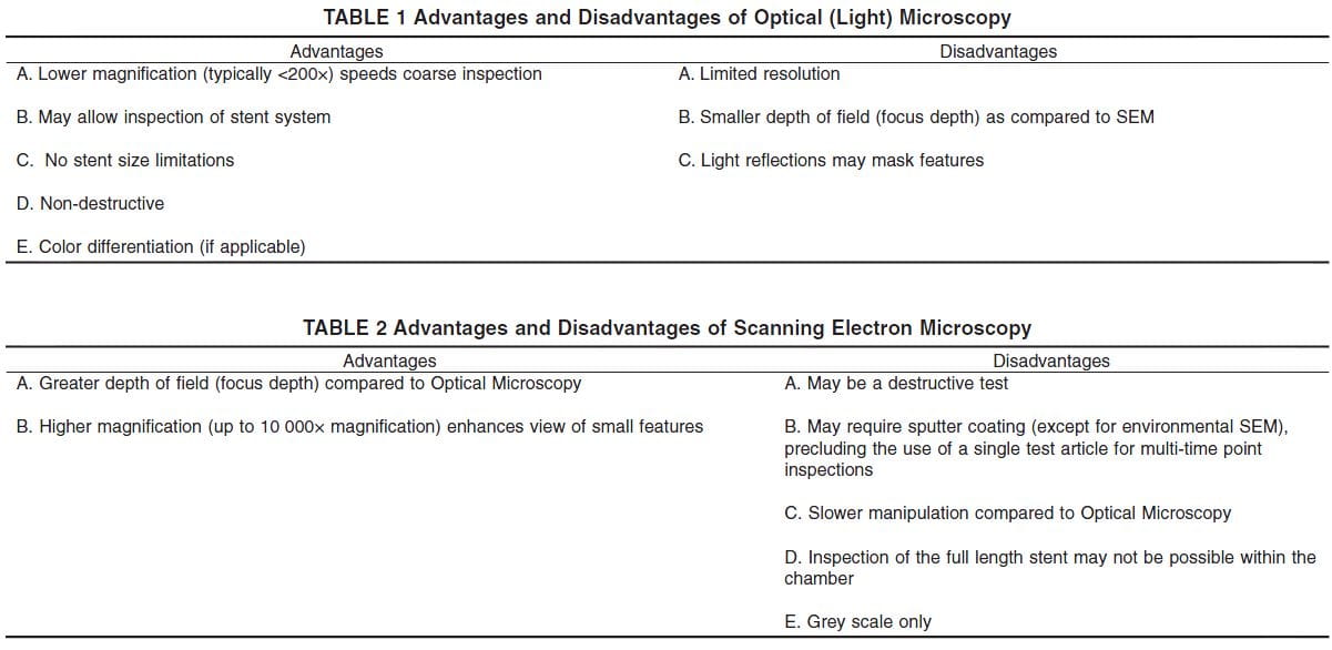
Advantages and Disadvantages
Optical microscopy is an ideal method for general inspection purposes, but scanning electron microscopy can provide the user with incredibly detailed topographical and compositional information. A scanning electron microscope typically features three types of detectors: a Secondary Electron Detector (SED), a Back-Scattered Electron Detector (BSED), and an Energy Dispersive Spectrum Detector (EDS).
The SED provides detailed topographical information to the user since secondary electrons interact primarily with the sample surface and have a large reflection angle, while the BSED provides both basic topographical and basic compositional information to the user since back-scattered electrons penetrate further into the material, and have a smaller reflection angle. The compositional data is relative – low-atomic-number materials appear dark and high-atomic number materials appear light in the SEM, but the exact chemical composition cannot be provided by the BSED.

The EDS provides detailed chemical compositional information. In some cases, it is beneficial to use scanning electron microscopy as a secondary inspection method. First, optical microscopy is used to observe gross defects. The specimen can be easily maneuvered using this method, and all gross defects can be charted and documented relatively quickly for further review. Next, scanning electron microscopy is used to observe the charted gross defects in more detail and to observe micro-defects not visible with optical microscopy. This two-phase approach combines the benefits associated with each inspection method and provides the customer with a more detailed inspection in less time (as compared to an SEM-only full-surface inspection).
Element has an Aspex Model 3025 SEM system with Automated Feature Analysis (AFA) Software and EDS (Energy Dispersive Spectrum) capabilities. The system is used for the inspection of defects on medical devices as well as particulate analysis studies. For the later, particulates shed from the device are captured on gold or carbon plated filters and up to 6 filters are placed in the SEM for subsequent analysis. The AFA software analyzes each filter individually and gathers a considerable amount of data on each particle.
Conclusions
Optical Microscopy and Scanning Electron Microscopy are fundamental inspection methods in the medical device industry, and Element offers both capabilities. Each has advantages and disadvantages, and our test engineers will help you determine which is most appropriate for your test needs. When combined with our extensive testing knowledge, you can feel confident that the inspection data provided by Element is the best available in the industry.
Find related Resources


