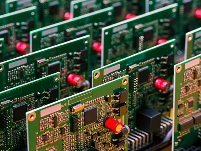
PCB Inspection & X-ray Analysis
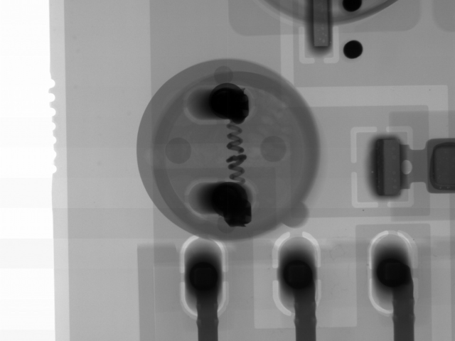
Element helps manufacturers evaluate PCB assembly quality through inspection-led X-ray analysis. This service supports non-destructive evaluation of solder joints, BGAs, and interconnects, with supporting microsection and analytical methods where required. Designed for inspection and verification needs, this capability provides insight into assembly quality without the scope of full PCB qualification testing.
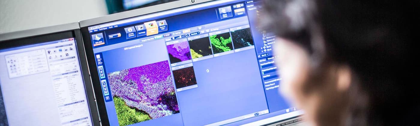
What is PCB X-ray Inspection at Element?
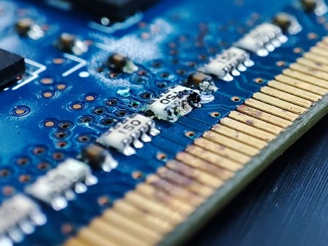
PCB X-ray Inspection is used to evaluate the quality and integrity of printed circuit board assemblies at the inspection stage without damaging the product. X-ray inspection allows internal features such as solder joints and BGAs to be examined for voiding, defects, and acceptability.
At Element, this service focuses on inspection-stage evaluation, supported by microsection and analytical techniques where required, as part of Element’s broader Printed Circuit Board (PCB) Testing services, to help customers make informed quality and acceptance decisions.

What Can Element Offer You For PCB X-Ray Inspection
Components and Materials We Test
Components and Materials We Test
Printed circuit boards (PCBs)
- Printed circuit board assemblies (PCBAs)
- Solder joints and interconnects
- Ball grid arrays (BGAs)
- Surface mount devices (SMDs)
- Through-hole components
- Leaded and lead-free solder materials
Key Tests Offered
Key Tests Offered
- PCB X-ray inspection for solder joints and BGAs
- Void percentage analysis
- IPC-A-610 visual inspection
- Dye and pry analysis
- Supporting microsection analysis
Methods and Solutions Offered
Methods and Solutions Offered
- Non-destructive X-ray inspection
- Visual inspection and dissection
- Cross-section and microsection analysis
- SEM/EDS analysis for solder and materials evaluation
- Related non-destructive testing (NDT) services where broader evaluation is required
Cutting-Edge Equipment We Use
Cutting-Edge Equipment We Use
- Advanced X-ray inspection systems with CT-style capabilities
- Digital microscopy for PCB inspection
- Precision microsection preparation equipment
Which Element Labs Offer This Service
Which Element Labs Offer This Service
Standards we test to and components we test
- IPC-A-610
- ASTM B827
- ASTM B845
- EIA-364-65-TP-65B
- ISO/IEC 60068-2-20
- Printed circuit boards (PCBs)
- PCB assemblies (PCBAs)
- Solder joints and interconnects
- Ball grid arrays (BGAs)
Your Challenges, Our Solutions
Hidden solder defects
Limited inspection visibility
Acceptability uncertainty
Targeted inspection needs
Element Experts at your service

Why Choose Element
Inspection-led focus
Advanced X-ray capability
IPC-certified expertise
Integrated analysis
Frequently asked questions
What is PCB X-ray inspection used for?
PCB X-ray inspection is used to assess internal features of PCB assemblies that cannot be evaluated through visual inspection alone. It supports the identification of solder joint voiding, misalignment, and other internal conditions that may affect assembly quality.
How is PCB inspection different from PCB testing?
PCB inspection is focused on evaluating assembly quality and acceptability at specific points in manufacturing. PCB testing typically includes broader qualification, reliability, or performance assessments conducted across additional lifecycle stages.
When is X-ray inspection preferred over cross-section analysis?
X-ray inspection is preferred when non-destructive evaluation is required or when multiple locations on a PCB need to be reviewed efficiently. Cross-section analysis may be used as a supporting method when detailed confirmation of internal structures is needed.
What standards are used for PCB inspection and X-ray analysis?
PCB inspection and X-ray analysis may be performed to applicable inspection and materials-related standards, such as IPC-A-610, depending on inspection objectives and customer requirements.

Explore our global network of labs and find your nearest location
VIEW ALL LOCATIONSRelated Services
Printed Circuit Board (PCB) Testing
Looking for reliable printed circuit board testing? Element ensures PCB and assembly quality with advanced HATS2â„¢, counterfeit detection, and compliance. Learn More.

PCB Cross-Section (Microsection) Analysis
Ensure the integrity of your printed circuit boards with Element's expert PCB microsectioning & cross-section analysis. Precise results & industry-leading turnaround times.
PCB Cleanliness & Contamination Testing
Ensure product reliability with Element's PCB Cleanliness & Contamination Testing. Our FTIR, IC, ROSE, and SEM/EDS analyses identify contaminants before they cause failures. Fast results from North America's PCB experts.
Printed Circuit Board (PCB) Failure Analysis
Understand and rectify the root causes of PCB failure with industry-leading PCB failure analysis from the testing experts at Element. Optimize your PCB designs while managing costs. Learn More.