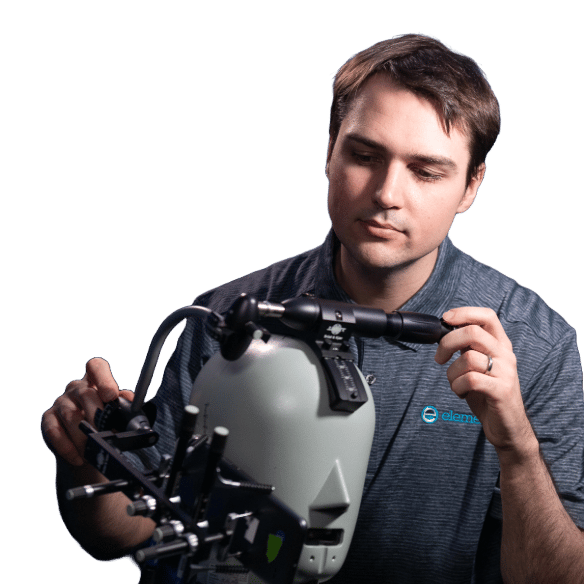
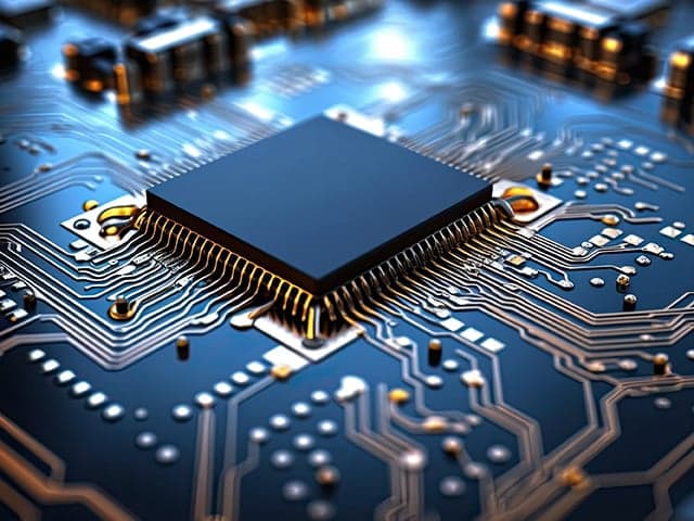
Surface Insulation Resistance (SIR) Testing
Meet demanding miniaturization challenges while ensuring PCB reliability with Element's Surface Insulation Resistance (SIR) Testing. As PCBs become smaller and spacing between their conductive parts decreases, our hands-on experts provide detailed insights into your PCB’s performance under real-world temperature and humidity conditions, helping you validate processes and prevent electrochemical failures. With rapid turnaround times and comprehensive analysis, we help you deliver superior products that meet rigorous reliability standards.

What is Surface Insulation Resistance (SIR) Testing at Element?
Surface insulation resistance (SIR) testing, also referred to as temperature humidity bias (THB) testing, is a test process used to determine if a printed circuit board is likely to fail when exposed to various temperature and humidity conditions.
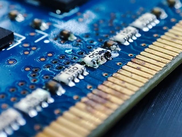
As PCBs become smaller and the spacing between their conductive parts decreases, they become more susceptible to failure modes caused by surface residues and humidity. Get detailed insights into your PCB's performance with our Surface Insulation Resistance testing, also known as temperature humidity bias (THB) testing. We simulate real-world conditions to identify potential failure modes like conductive anodic filament (CAF) formation and electrochemical migration and validate the effect of new processes on the product’s surface insulation resistance.
Why partner with Element for Surface Insulation Resistance (SIR) Testing?
Methods and solutions offered
Methods and solutions offered
Element's comprehensive approach to SIR testing includes controlled temperature and humidity exposure, real-time electrical attribute evaluation, and accelerated environmental testing. We help select and implement the most appropriate methodology based on your product and intended use, ensuring thorough validation of assembly processes, soldering fluxes, cleaning processes, and surface insulation resistance.
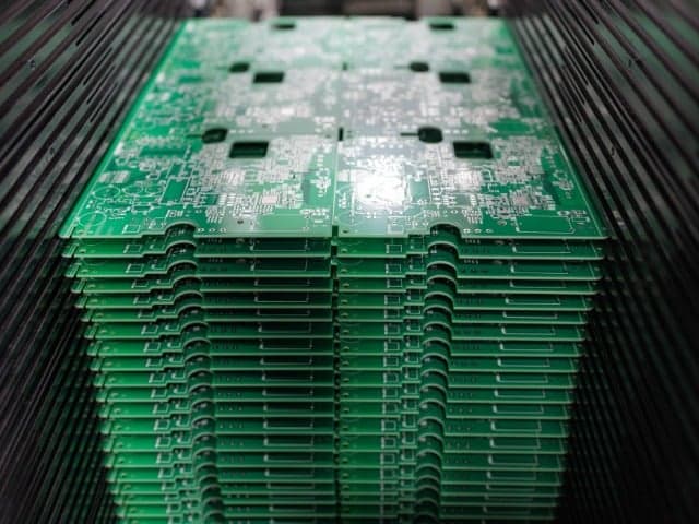
Components and materials we test
Components and materials we test
We test printed circuit boards of all sizes, focusing on spacing between conductive parts, surface residues, and humidity interaction points. Our testing validates both new and existing PCB assemblies, soldering fluxes, and cleaning processes to ensure optimal performance under varied environmental conditions.
Which labs offer this service
Which labs offer this service
Notably among our circuit board testing labs worldwide, our Anaheim, CA and Baltimore, MD labs, formerly known as Microtek and Trace Labs, have more than 30 years of experience partnering with leading OEMs and manufacturers.
Materials we test
Your Challenges, Our Solutions
Miniaturization Demands
Extreme Environment Performance
Process Validation
Surface Contamination Risks
Why Choose Element
Industry-Leading Experience
Knowledge of PCB Trends
Comprehensive Analysis
Hands-On Support
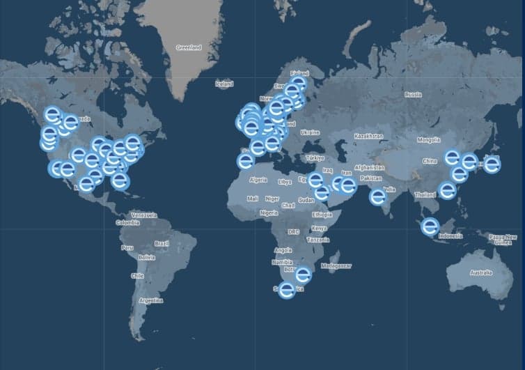
Explore our global network of labs and find your nearest location
VIEW ALL LOCATIONSRelated Resources
Related services
Printed Circuit Board (PCB) Testing
Looking for reliable printed circuit board testing? Element ensures PCB and assembly quality with advanced HATS2â„¢, counterfeit detection, and compliance. Learn More.
Printed Circuit Board (PCB) Failure Analysis
Understand and rectify the root causes of PCB failure with industry-leading PCB failure analysis from the testing experts at Element. Optimize your PCB designs while managing costs. Learn More.
Failure Analysis for Electronic Devices & Components Services
Element's comprehensive failure analysis services help you identify root causes, prevent future failures, and protect your brand reputation.
Electromagnetic Compatibility (EMC) Testing & Electromagnetic Interference (EMI) Testing & Certification
Element provides accredited EMC and EMI testing and certification services, helping businesses meet regulatory requirements, reduce costly redesigns, and bring products to market faster through expert compliance support.